

Single Sided Copper Clad 70mm*100mm PRO45 ,R13
$ 1.23
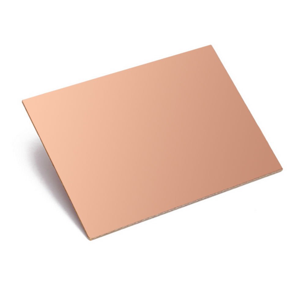
DescriptionWhen a prototype proves successful, it is time to make it permanent. The Single Sided Copper Clad Board empowers you to manufacture your own Printed Circuit Boards (PCBs) at home or in the lab. Instead of waiting weeks for overseas fabrication houses to manufacture and ship your design, you can rapidly prototype and test a custom hardware layout in a single afternoon.The Etching CanvasThis board is essentially a completely blank circuit. The entire top surface is coated in a thin, highly conductive layer of copper. To create your circuit, you must selectively remove the copper you do not want, leaving behind the precise “traces” (wires) that connect your components.Popular Fabrication Methods:Chemical Etching: The most common DIY method. You print your circuit design onto glossy paper using a laser printer, iron the toner directly onto the copper, and submerge the board in an etchant solution (like Ferric Chloride or a Vinegar/Peroxide mix). The toner protects your traces, while the exposed copper dissolves away.CNC Milling: If you have access to a desktop CNC router, you can use a V-bit to mechanically carve away the copper outlines, creating beautifully precise isolation traces without dealing with messy chemicals.The “Sharpie” Method: For incredibly simple, low-complexity circuits, you can literally draw your traces directly onto the copper using a permanent marker before dipping it into an acid bath.High-Quality FR-4 BaseNot all blank PCBs are created equal. Cheaper boards use a paper-phenolic base that snaps easily and burns under a soldering iron. This board utilizes a standard FR-4 Fiberglass Epoxy substrate. It is incredibly rigid, flame-resistant, and can withstand repeated, high-temperature hand soldering without the copper pads peeling away from the base material.Single-Sided SimplicityBecause this board is single-sided (copper on one side, bare fiberglass on the other), it is exceptionally beginner-friendly. It is perfect for designing through-hole circuits where components sit on the bare top side, and their legs are soldered to the copper traces on the bottom.Key Features:Rapid Prototyping: Turn a schematic into a physical, working circuit board in a matter of hours.Easy to Cut: The 70x100mm footprint can be easily scored with a heavy-duty craft knife and snapped, or cut with a standard hacksaw to create smaller, custom-sized modules.Excellent Conductivity: The pure copper layer ensures low-resistance power delivery and clean signal routing.Technical Specifications:Dimensions: 70mm x 100mmSides: Single-SidedSubstrate Material: FR-4 (Woven glass and epoxy)Conductive Layer: CopperBoard Thickness: ~1.2mm – 1.6mmIdeal Applications:In-house rapid prototyping of custom Arduino shields and IoT sensor boardsBuilding heavy-duty power distribution boards (where you can leave massive, wide copper traces to carry high current)Creating custom RF antennas and ground planesEducational workshops teaching the fundamentals of PCB design and fabrication